101ifos-2019-subject-08-002
Paper II15 Marks
Explain the Meissner effect in superconductivity. Obtain an expression for London penetration depth of magnetic field for a superconductor.
Search, filter, and study UPSC Civil Services & IFoS Physics past year questions with rigorous derivations, formulas, and step-by-step solutions.
Buy PYQ Solution Manual →
Explain the Meissner effect in superconductivity. Obtain an expression for London penetration depth of magnetic field for a superconductor.
A silicon semiconductor sample at T=300\,\mathrm{K} having cross-sectional area of 0.5\,\mu\mathrm{m}^2 has a pentavalent donor doping profile given by C(x)=5\times10^{16}e^{-x/L_n}\,\mathrm{cm^{-3}}. Given, the mobility of the electrons in the sample is 1250\,\mathrm{cm^2\,V^{-1}\,s^{-1}} and the diffusion length of the electrons, L_n, is 4\,\mu\mathrm{m}. Calculate the diffusion current in the sample at distance x=2\,\mu\mathrm{m}.
Sketch the cross-sectional structure of an enhancement mode MOSFET and explain its principles of operation with the help of its output characteristics.
An n-channel silicon JFET has donor concentration of 2 \times 10^{21}/\text{m}^3 and a channel width of 4~\mu\text{m}. If the dielectric constant of silicon is 12, find the pinch-off voltage. If the FET operates with a gate-source voltage of -2~\text{V}, what is the saturation voltage V_{\text{Dsat}}?
Explain the use of an op-amp as a differentiator and an integrator using proper circuit diagram. Write the condition to work as good differentiator and integrator.
A transistor having \alpha = 0\cdot 975 and a reverse saturation current I_{\text{CO}} = 10~\mu\text{A} is operated in CE configuration. What is \beta for this configuration? If the base current is 250~\mu\text{A}, calculate the emitter current and the collector current.
Describe briefly the construction of an enhancement type MOSFET using a p-type silicon bar. Point out the structural difference between enhancement and depletion forms of the MOSFET.
A silicon semiconductor sample is doped with 6\times10^{16}\,\mathrm{cm^{-3}} of aluminium and 7\times10^{15}\,\mathrm{cm^{-3}} of phosphorus atoms. Given at T=300\,\mathrm{K}, the intrinsic carrier concentration, n_i=1.5\times10^{10}\,\mathrm{cm^{-3}}; the band gap, E_g=1.1\,\mathrm{eV}; the electron mobility, \mu_n=1250\,\mathrm{cm^2\,V^{-1}\,s^{-1}} and the hole mobility, \mu_p=480\,\mathrm{cm^2\,V^{-1}\,s^{-1}}. Determine in the sample of the following:
(i) The type of the semiconductor, n or p
(ii) The hole carrier concentration
(iii) The electron carrier concentration
(iv) The position of the Fermi level in the sample with respect to the bottom of the conduction band
(v) The conductivity of the sample
A 5\,\mathrm{cm^2} Ge solar cell with a dark reverse saturation current of 2\,\mathrm{nA} has solar radiation incident upon it, producing 4\times10^{17} electron-hole pairs per second. The electron and hole diffusion lengths are given to be 5\,\mu\mathrm{m} and 2\,\mu\mathrm{m}, respectively. Calculate for the cell of the following:
(i) The short-circuit current
(ii) The open-circuit voltage
Obtain the Boolean expression for the output Y in the given logic circuit :
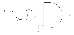
Simplify the expression and show that the circuit is equivalent to an AND gate with inputs A and B.
Consider a face-centred cubic lattice of side a. Deduce --
(i) The primitive translation vectors;
(ii) The volume of the primitive cell;
(iii) The reciprocal primitive translation vectors;
(iv) The volume of the reciprocal lattice
A small magnet is placed on the surface of a disc of normal material. Explain what happens when the disc is cooled down so that it becomes superconducting. Can this be explained from classical viewpoint if we simply treat the superconductor as a material which has zero resistivity ?
What are type I and type II superconductors? Give examples. Discuss and compare Meissner effect and perfect diamagnetic behaviour for type I and type II superconductors.
Calculate the total conductivity in an intrinsic semiconductor. How does this conductivity change with temperature ?
Draw the circuit of a phase shift oscillator using transistor. Obtain the expression for the frequency of oscillations and condition for sustained oscillations. Give necessary equivalent circuit while deriving the expression of frequency of oscillations and condition for sustained oscillations.
Explain drift velocity, mobility and conductivity of an intrinsic semiconductor.
Derive the expression for electron concentration in the conduction band of an intrinsic semiconductor.
A pair of transistors operates in a class B push-pull circuit with a power supply of voltage V_{\text{cc}} = 12\text{ V}. If the turns ratio of the output transformer is 2 and the load resistance R_{\text{L}} is 6\ \Omega, calculate the maximum output power and maximum dc power supplied. Hence find efficiency of the circuit. Neglect transformer winding resistance.
What are intrinsic and extrinsic semiconductors? Show that in the intrinsic semiconductors, Fermi level lies exactly in the middle of bottom of conduction band and top of valence band.
Calculate Atomic Packing Fraction (APF) for FCC and HCP structures, and show that these are the most closely packed structures.