Considering the electrons in the atom, what is the difference between a diamagnetic and a paramagnetic substance? State how magnetic the susceptibility varies with temperature for dia, para, ferro- and anti-ferro-magnetic materials. (No theoretical discussion required.)
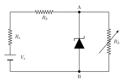
What is a Zener diode? Explain what function it performs in the circuit given below as the load resistance R_L is varied. What is the purpose of introducing resistor R_2 in the circuit? (V_s and R_s represent source voltage and resistance, respectively).
What is a P.N. junction? Describe with energy level diagram the formation of double layer of charges which generates a potential difference (V) across, the junction. Hence show that the capacitance of the double layer. C=KV^{-1/2}, where K is a constant. State some practical use of this relation between C and V.
Draw the circuit diagrams suitable for measuring the voltage amplification of a triode valve with the following methods of connection: (a) Common cathode (b) Common grid (c) Common anode. Write down, without proofs, the expression for amplification in each case in terms of \mu and the relevant resistance values. Which of the three methods is usually employed in high frequency circuit practices and why ?
Write a shout note (about 200 words) on super-conductors and the nature of revolution that may come up if superconductors with critical temperature well above the room temperatures are developed.
Define Fermi energy. Show that the Fermi level lays half-way between the top of the valence band and the bottom of the conduction band of an intrinsic semiconductor. Explain why an extrinsic semiconductor, such as an N-type crystal, has more free electrons than holes but is found to be electrically uncharged.
Give an account of the basic principles of radio transmission and reception. Detailed circuits are not necessary but schematic diagrams indicating functions of various units may be shown.
A triode has a transconductance (g_m) of 1,600\text{ micromhos}. The following table gives two sets of the plate voltage (E_b), the grid voltage (E_c) and the plate current (I_b). \begin{tabular}{c c c} E_b & E_c & I_b \\ 250\text{ V} & -22\text{ V} & 12.6\text{ mA} \\ 180 & -16.5 & 12.0 \end{tabular} Define the terms amplification factor and plate resistance and calculate them for the above case.
Draw a complete circuit for common emitter (small signal) amplifier for low frequencies and explain briefly its working.
Explain, on the basis of bond structure, the behaviour of insulators and conductors. Describe the effect of adding donor or acceptor impurities on conduction in a semi-conductor. Explain the action of a p-n junction as a rectifier. \begin{aligned} \text{Mass of electron} &= 9.1 \times 10^{-31}\text{ kg} \\\\ 1\text{ a.m.u} &= 931\text{ MeV} \\\\ \text{Avogadro's numbers} &= 6.1 \times 10^{23}\text{ (gm-mole)}^{-1} \\\\ \varepsilon_0 &= 1/36\pi \times 10^{-9}\text{ f/m} \\\\ h &= 6.6 \times 10^{-27}\text{ erg sec} \\\\ c &= 3.0 \times 10^{10}\text{ cm/sec} \\\\ 1\text{ eV} &= 1.6 \times 10^{-19}\text{ erg} \\\\ &= 1.6 \times 10^{-19}\text{ joule} \end{aligned}
Distinguish between dia-, para- and ferromagnetism. Give an account of Weiss theory of ferromagnetism.
Give the basic structure of a n-channel depletion type MOSFET. Draw the drain current-drain voltage characteristics both in depletion as well as in enhancement modes.
Why are NAND and NOR gates called universal gates? Give the logic diagram, Boolean equation and the truth table of NAND gate. Design an OR gate using only NAND gates.